- 您现在的位置:买卖IC网 > Sheet目录477 > MICRF022YM-FS12 (Micrel Inc)IC RECEIVER ASK 300-440MHZ 8SOIC
�� �
�
�Micrel,� Inc.�
�C� AGC� Pin�
�VDDBB�
�MICRF002/RF022�
�driver� is� recommended� for� driving� high-capacitance� loads.�
�REFOSC� Pin�
�Compa-�
�rator�
�1.5μA�
�67.5μA�
�REFOSC�
�30pF�
�Active�
�Bias�
�200k�
�250�
�VDDBB�
�CAGC�
�30pF�
�30μA�
�Timout�
�15μA�
�675μA�
�VSSBB�
�VSSBB�
�Figure� 5.� REFOSC� Pin�
�VSSBB�
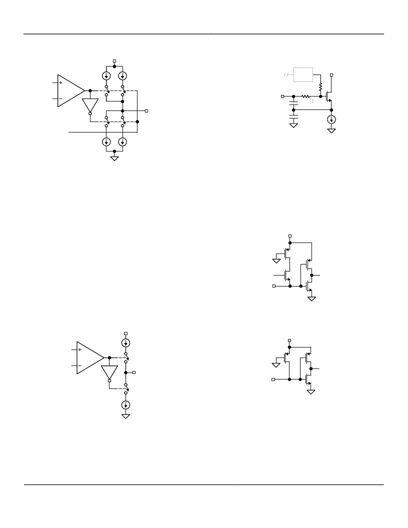
�Figure� 3.� CAGC� Pin�
�Figure� 3� illustrates� the� C� AGC� pin� interface� circuit.� The� AGC�
�control� voltage� is� developed� as� an� integrated� current� into� a�
�capacitor� C� AGC� .� The� attack� current� is� nominally� 15� μ� A,� while�
�the� decay� current� is� a� 1/10th� scaling� of� this,� nominally�
�1.5� μ� A,� making� the� attack/decay� time� constant� ratio� a� fixed�
�10:1.� Signal� gain� of� the� RF/IF� strip� inside� the� IC� diminishes�
�as� the� voltage� at� C� AGC� decreases.� Modification� of� the�
�attack/decay� ratio� is� possible� by� adding� resistance� from� the�
�C� AGC� pin� to� either� V� DDBB� or� V� SSBB� ,� as� desired.�
�The� REFOSC� input� circuit� is� shown� in� Figure� 5.� Input�
�impedance� is� high� (200k� ?� ).� This� is� a� Colpitts� oscillator� with�
�internal� 30pF� capacitors.� This� input� is� intended� to� work� with�
�standard� ceramic� resonators� connected� from� this� pin� to� the�
�V� SSBB� pin,� although� a� crystal� may� be� used� when� greater�
�frequency� accuracy� is� required.� The� nominal� dc� bias�
�voltage� on� this� pin� is� 1.4V.�
�SEL0,� SEL1,� SWEN,� and� SHUT� Pins�
�VDDBB�
�Q1�
�Both� the� push� and� pull� current� sources� are� disabled� during�
�shutdown,� which� maintains� the� voltage� across� C� AGC� ,� and�
�improves� recovery� time� in� duty-cycled� applications.� To�
�further� improve� duty-cycle� recovery,� both� push� and� pull�
�currents� are� increased� by� 45� times� for� approximately� 10ms�
�after� release� of� the� SHUT� pin.� This� allows� rapid� recovery� of�
�any� voltage� droop� on� C� AGC� while� in� shutdown.�
�VSSBB�
�SHUT�
�SEL0,�
�SEL1,�
�SWEN�
�Q4�
�Q2�
�to� Internal�
�Circuits�
�Q3�
�VSSBB�
�DO� and� WAKEB� Pins�
�VDDBB�
�10μA�
�Figure� 6a.� SEL0,� SEL1,� SWEN� Pins�
�VDDBB�
�Compa-�
�rator�
�DO�
�VSSBB�
�SHUT�
�Q1�
�Q2�
�Q3�
�to� Internal�
�Circuits�
�VSSBB�
�10μA�
�Figure� 6b.� SHUT� Pin�
�VSSBB�
�Figure� 4.� DO� and� WAKEB� Pins�
�The� output� stage� for� DO� (digital� output)� and� WAKEB�
�(wakeup� output)� is� shown� in� Figure� 4.� The� output� is� a� 10� μ� A�
�push� and� 10� μ� A� pull� switched-current� stage.� This� output�
�stage� is� capable� of� driving� CMOS� loads.� An� external� buffer-�
�Control� input� circuitry� is� shown� in� Figures� 6a� and� 6b.� The�
�standard� input� is� a� logic� inverter� constructed� with� minimum�
�geometry� MOSFETs� (Q2,� Q3).� P-channel� MOSFET� Q1� is�
�a� large� channel� length� device� which� functions� essentially�
�as� a� “weak”� pullup� to� V� DDBB� .� Typical� pull-up� current� is� 5� μ� A,�
�leading� to� an� impedance� to� the� V� DDBB� supply� of� typically�
�1M� ?� .�
�July� 2008�
�13�
�M9999-070808�
�发布紧急采购,3分钟左右您将得到回复。
相关PDF资料
MICRF211AYQS TR
IC RCVR 3V 433.92MHZ 16-QSOP
MICRF213AYQS TR
IC RX 3.3V 300-350 MHZ 16QSOP
MICRF218AYQS TR
IC RCVR QWIKRADIO 3.3V 16QSOP
MICRF219AAYQS TR
IC RECEIVER QWIKRADIO 16QSOP
MICRF219AYQS TR
IC RECEIVER QWIKRADIO 16QSOP
MICRF220AYQS TR
RCVR ASK/OOK 300-450MHZ 16QSOP
MICRF221AYQS TR
IC RF RECEIVER QWIKRADIO 16-QSOP
MICRF300YC6 TR
IC AMP 100/1000MHZ LN SC70-6
相关代理商/技术参数
MICRF022YM-FS12 TR
功能描述:射频接收器 300-440MHz RF Receiver With Shutdown( Lead Free)
RoHS:否 制造商:Skyworks Solutions, Inc. 类型:GPS Receiver 封装 / 箱体:QFN-24 工作频率:4.092 MHz 工作电源电压:3.3 V 封装:Reel
MICRF022YM-FS24
功能描述:射频接收器 300-440MHz RF Receiver With Shutdown( Lead Free)
RoHS:否 制造商:Skyworks Solutions, Inc. 类型:GPS Receiver 封装 / 箱体:QFN-24 工作频率:4.092 MHz 工作电源电压:3.3 V 封装:Reel
MICRF022YM-FS24 TR
功能描述:射频接收器 300-440MHz RF Receiver With Shutdown( Lead Free)
RoHS:否 制造商:Skyworks Solutions, Inc. 类型:GPS Receiver 封装 / 箱体:QFN-24 工作频率:4.092 MHz 工作电源电压:3.3 V 封装:Reel
MICRF022YM-FS48
功能描述:射频接收器 300-440MHz RF Receiver With Shutdown( Lead Free)
RoHS:否 制造商:Skyworks Solutions, Inc. 类型:GPS Receiver 封装 / 箱体:QFN-24 工作频率:4.092 MHz 工作电源电压:3.3 V 封装:Reel
MICRF022YM-FS48 TR
功能描述:射频接收器 300-440MHz RF Receiver With Shutdown( Lead Free)
RoHS:否 制造商:Skyworks Solutions, Inc. 类型:GPS Receiver 封装 / 箱体:QFN-24 工作频率:4.092 MHz 工作电源电压:3.3 V 封装:Reel
MICRF022YM-SW48
制造商:MICREL 制造商全称:Micrel Semiconductor 功能描述:300-440MHz QwikRadio? ASK Receiver
MICRF033BM
制造商:Micrel Inc 功能描述:RF Receiver 5V 8-Pin SOIC 制造商:Rochester Electronics LLC 功能描述:- Bulk
MICRF102
制造商:MICREL 制造商全称:Micrel Semiconductor 功能描述:QwikRadio UHF ASK Transmitter